QMM Lab banner

Research Topics

Vectorial nanocurrents

Currents of all kinds result from broken symmetries, in space or in time. Charge currents that arise in the presence of applied electric fields (which define a specific flow direction) serve as the basis for most modern technologies and powerful scientific probes of material properties. Ultrafast light pulses can also drive photocurrents in materials on timescales several orders of magnitude faster applied voltages, yet these rely either on intrinsically broken symmetries of the material lattice or extrinsic symmetry breaking at interfaces, since electromagnetic light fields oscillate back and forth rapidly with zero net directionality. Several methods have emerged recently that exploit nonlinearity to controllably drive currents in symmetric materials, yet these rely on phase-sensitive setups that are difficult to spatially pattern or scale up. So how can we proceed?

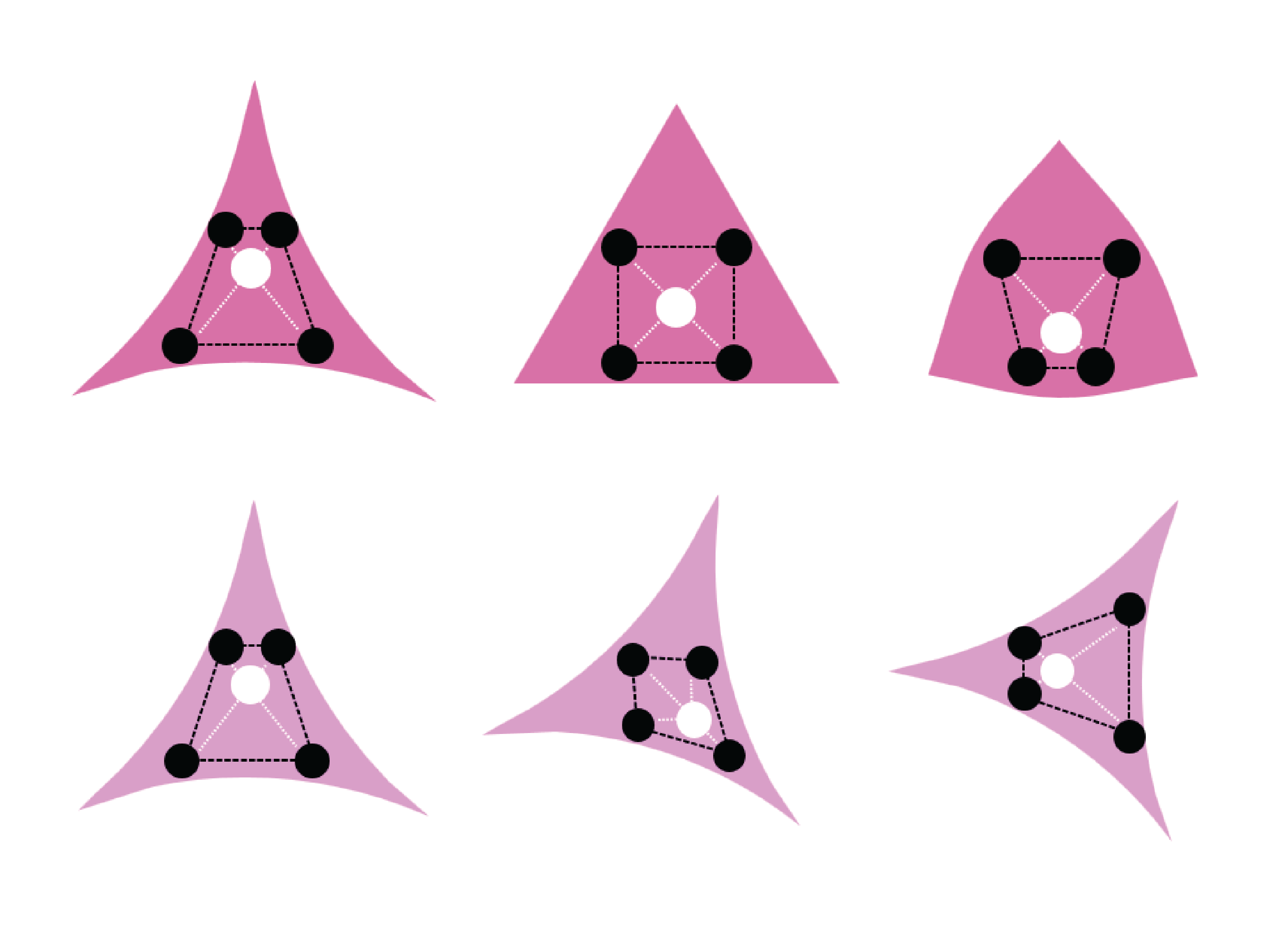
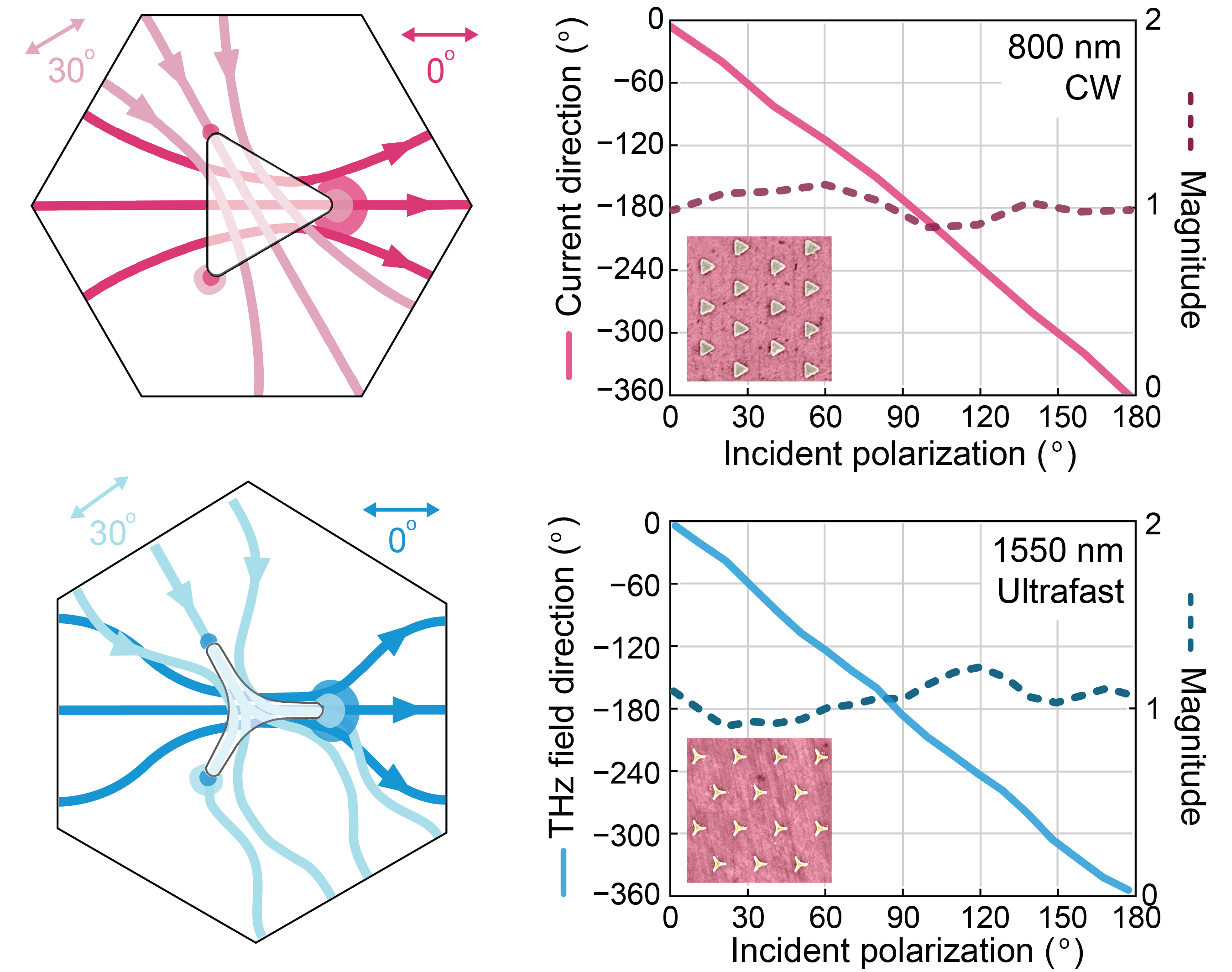
A remarkably simple and versatile option turns out to be: Pattern extrinsic structure with the desired symmetry directly onto or into the material. With symmetry-broken plasmonic (e.g., gold) metasurfaces on otherwise centrosymmetric graphene, for instance, we can drive strong nanoscale charge flow with directional structures. Furthermore, the light-matter interaction can define an arbitrary directionality with triangular structures that are inversion-broken but not inherently directional. This leads to broad capabilities for patterning and dynamically controlling ultrafast, nanoscale charge flow in many different materials.

Recently, we have demonstrated that symmetry-engineered nanocurrents can be used as a new space-, time-, and angle-resolved photocurrent probe of material properties. In simple device geometries they directly reveal the intrinsic equipotential and electric field lines of the device, while in the presence of spatial inhomogeneity they can be used to map domain structure due to deviations in these flow lines and the magnitude of the local response. Another application that emerges is structured terahertz light, and we have discovered that optically tunable compressive (radial) and circulating (azimuthal) photocurrents emit special light pulses that carry nontrivial topology (see 'Topological light'). Other possibilities for optoelectronic signal transduction and adaptive interconnects in classical and quantum information systems are presently under investigation.

Image: Triangular nanostructures yielding current flow that can be driven in any direction, simply by rotating the linear polarization of the incident optical excitation laser. Results shown for gold nanotriangles (800 nm resonance) and tri-petal structures (1550 nm resonance) on graphene, serving as the basis for much broader applications in a variety of material platforms.
Designer superlattices

Moiré materials have emerged as versatile platforms for exploring topological and strongly-correlated phases, with the notable recent discoveries of unconventional superconductivity and fractional Chern insulators. Such states emerge around flat electronic minibands where Coulomb interactions exceed the kinetic energy, based on the nanoscale modulation of hopping between vdW layers. These superlattice geometries are constrained, however, by the underlying atomic lattices, while strain and stacking disorder can also obscure the essential physics for global probes. Drawing inspiration from moiré systems, the QMM Lab is developing complementary methods for generating untwisted vdW superlattices, instead exploiting precision nanopatterning to generate gauge potentials with high geometric tunability and uniformity across large device areas.

Graphene serves as a natural starting point, where electronic structure engineering has already been demonstrated in superlattices based on chemical modification, hole etching, electrostatic gating (see some exciting recent work in the Du Lab and Cano Group), and strain. Thus far, however, only periodically gated and strained graphene have displayed signatures of electronic correlations within the flat minibands. Under strain, the spatial modulation of hopping is represented by a gauge field that behaves just like an electromagnetic vector potential and yields massive pseudo-magnetic fields (hundreds of Tesla!) that can exceed the real fields available even in pulsed magnet facilities. Extremely flat topological minibands and emergent anomalous Hall phases have indeed been anticipated theoretically for some time in strained graphene by analogy with the perfectly flat Landau levels of a 2D electron gas in a real magnetic field, yet fabrication challenges have limited experimental advances. To overcome this, we have recently refined a high-resolution electron beam lithography process with spin-on glass, whereby nearly arbitrary height profiles can be patterned onto standard SiO2/Si device substrates with resolution down to the sub-20 nm scale of magic angle moiré superlattices. These specialized substrates offer both designer strain fields and periodic back-gates for overlaid 2D material stacks, including a conformal top gate for tuning chemical potential.

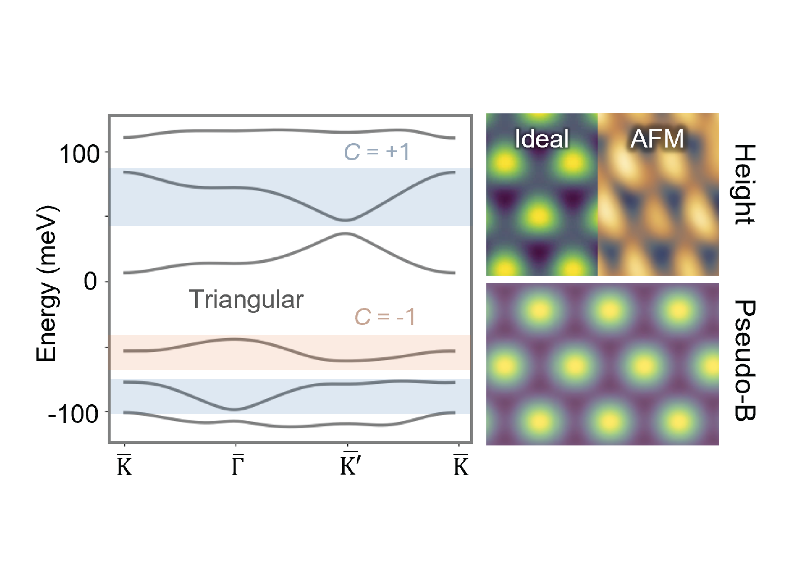
Continuum model calculations reveal highly modified electronic structure for hexagonal nano-strained superlattices, including flat minibands. To gap the system, isolate topological minibands, and thus prepare a nearly ideal setting for the emergence of quantum anomalous Hall and various correlated states, we further deform the nanodots into triangles. Crucially, while the inversion symmetry breaking leads to inequivalent spatial distributions of A and B sublattice polarization (with pseudo-magnetic fields polarizing this pseudo-spin degree of freedom), a matching scalar potential built into the periodic capacitance of our device geometry is needed to split these energies, induce a mass gap, and allow spontaneous valley polarization to break time reversal. Beyond triangular lattices, more exotic geometries such as frustrated kagome and Lieb lattices have flat bands encoded in their underlying tight binding descriptions, with the breathing kagome exhibiting a ladder of extremely flat and isolated minibands.

Image: Continuum tight-binding calculations of graphene strained on nanotriangular pillars (ideal and real height profiles shown), yielding flat and topological minibands.

Cavity physics

Strong terahertz fields can drive infrared active phonons and other collective excitations far out of equilibrium, leading to nonlinear couplings with Raman modes and net lattice distortions used to access metastable phases of matter. However, this relies on identifying suitable materials with modes strategically positioned for strong phonon-phonon coupling or other interactions, as well as sufficiently weak potential barriers to drive the system into new transient ground states. Cavities with large terahertz field enhancements introduce new degrees of tunability to loosen these constraints, enabling 10- to 20-fold or higher field enhancements (driving accessible electric fields into the MV/cm2 range and magnetic fields into the several-Tesla range!) that (i) transiently break symmetries to induce new phases, (ii) drive efficient nonlinear couplings, and (iii) strongly dress and shift mode frequencies to enhance linear coupling. In our group, we are placing materials such as van der Waals magnets on or beneath lithographically-defined terahertz cavities to strongly modify ground state properties and ultrafast dynamics. We are exploring strong-coupling induced polaritonic mode splittings and resulting mode-shift-induced magnon-phonon coupling in the van der Waals magnets. We are further investigating enhanced nonlinear coupling between infrared-active and Raman phonons that have been shown to drive metastable magnetization around the Néel temperature. In other materials such as CrSBr, terahertz-driven metamagnetic AFM-to-FM transitions become accessible with Tesla-scale fields, driving new ultrafast phases and modes.

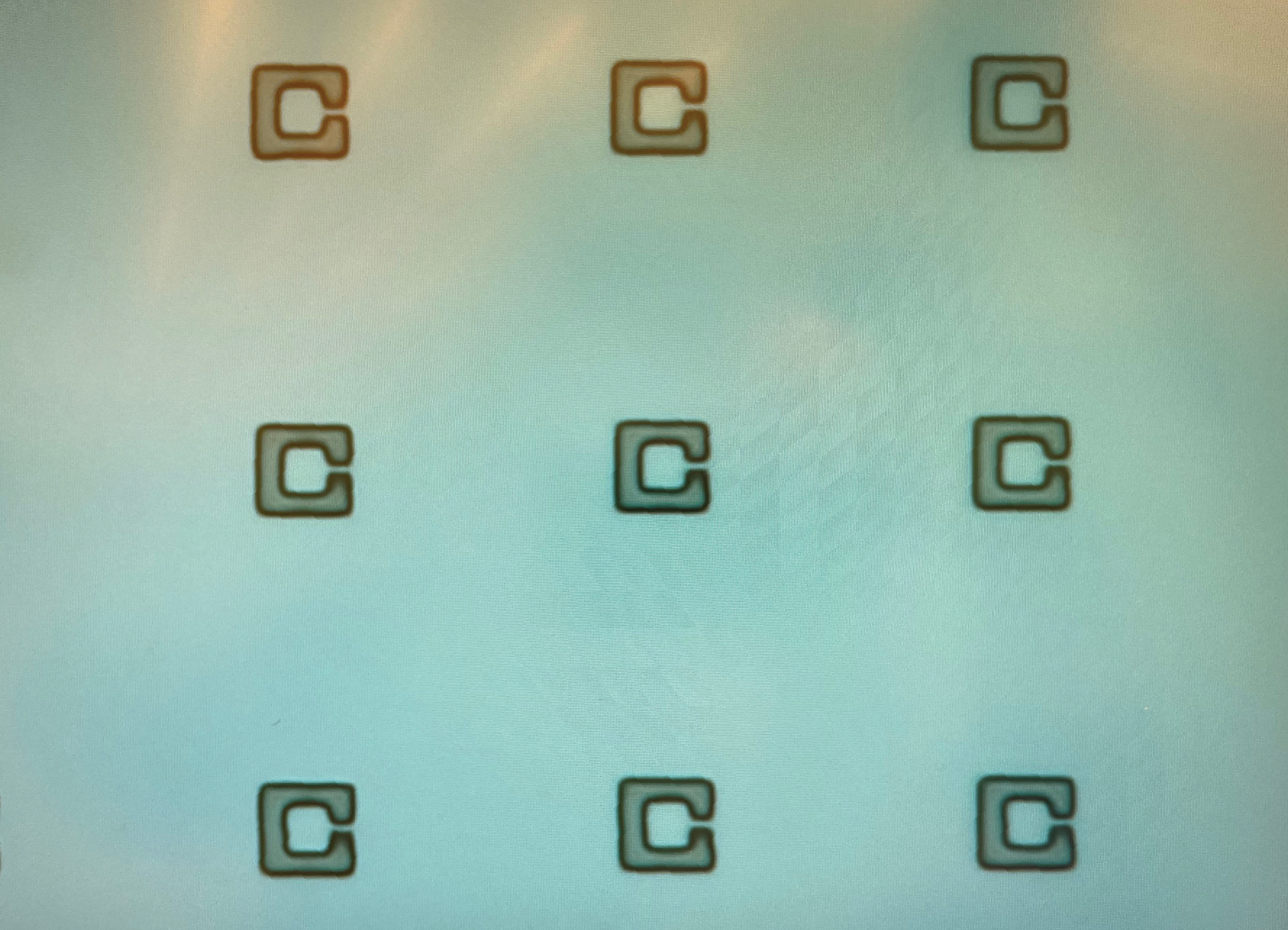
Image: Split-ring terahertz resonator array, with few-hundred-nanometer gaps that serve as the highly field-enhanced cavity region.

Nano-acoustic symmetry engineering

We are developing methods to nanostructure thin quantum materials, including films and flakes, and to excite acoustic structural modes of selected symmetries using ultrafast light pulses. Although such modes are well established in plasmonic metals, their implications for quantum materials and their ability to perturb intrinsic lattice symmetry remain largely unexplored. Because the symmetry of the nanostructure is imparted on the atomic lattice by the nano-acoustic strain field, this approach provides a versatile and deterministic route for exploring quantum-material phase diagrams, extending both static strain tuning and ultrafast nonlinear phononics. It enables dynamic breaking of lattice inversion symmetry through directional (C1) or triangular (C3) structural motifs, for example, which may provide access to topological phase transitions as well as chiral and multiferroic orders that otherwise remain deeply hidden to other ultrafast or static probes. We have already established the ability to pattern a wide range of thin films into well-defined nanostructures and have observed nano-acoustic modes in a quantum material for the first time, to our knowledge, specifically in the 2D ferromagnetic metal Fe3GeTe2. We are presently working to understand the implications for intrinsic material symmetries through techniques such as time-resolved second harmonic generation. Exploring the new class of nanostructured quantum matter is a timely and important problem, with the potential to advance the broader goal of materials by design and enable access to new magnetic, topological, and strongly correlated phases.

Image: Illustration of a nano-triangular acoustic mode distorting an underlying square lattice with transient directionality oscillating on hundreds-of-picosecond timescales (top). The local directionality is further controlled by the structure orientation (bottom).

Topological light

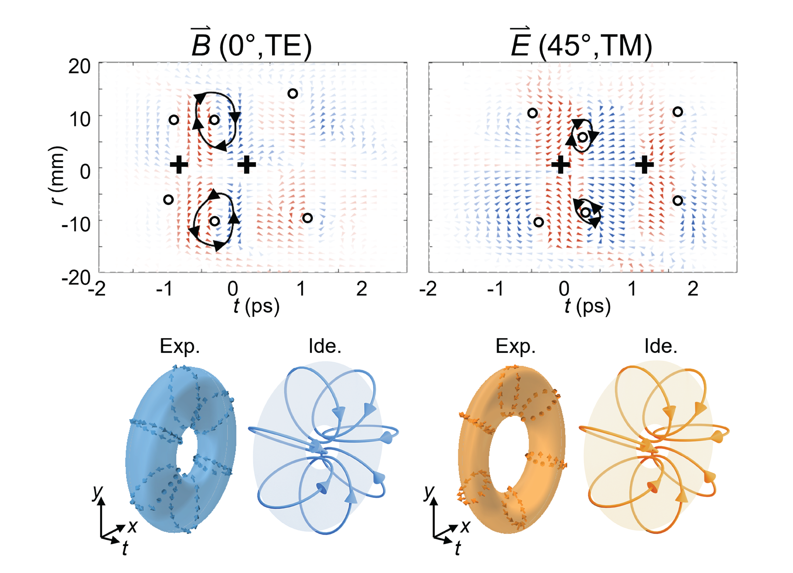
Photocurrents driven in materials by femtosecond-scale ultrafast light pulses often decay on sub-picosecond timescales due to momentum relaxing scattering with phonons. This change in currents leads to emission of electromagnetic radiation in the inverse-picosecond (or terahertz) spectral range. An unsurprising yet useful result is that the vectorial currents described above emit vectorial light fields in the terahertz spectral range. More surprising is that hyperspectral imaging reveals these fields to be a new and unusual form of toroidal light pulse, which carries skyrmion topology that evolves in space and time. While not truly topologically protected by an energy gap in the same sense as electronic states in condensed matter, these topological light pulses have proven to be highly robust against small perturbations. Furthermore, they have many degrees of freedom and higher-order modes in which for high-capacity information encoding. We are particularly exploring applications in materials science, where this form of terahertz light offers exciting new opportunities to probe difficult-to-access out-of-plane collective excitations (such as phonons and magnons) in van der Waals materials, along with toroidal modes and nonradiating dynamic anapole configurations.

Image: Azimuthal (left) and radial (right) electric field modes that yield magnetic and electric Néel-type skyrmions, respectively. The full 3D toroidal structure of the tunable topological light pulses is revealed by (hyperspectral) imaging of the terahertz waveform in space and time.

Experimental Approaches

Autonomous Transient Optical Microscopy (ATOM)

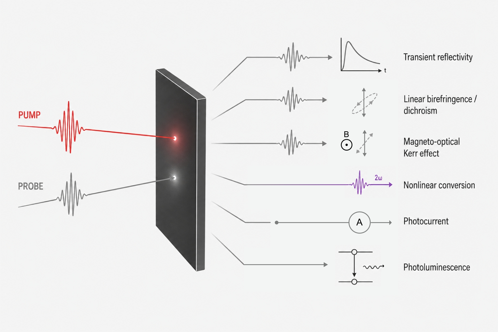
We are currently developing a highly automated system for ultrafast optical pump-probe microscopy and spectroscopy of quantum materials. Between the broad set of incident laser parameters (intensities, wavelengths, polarizations, positions, and time delay), quantum material properties and phases under different sample conditions (temperature, magnetic field vector, applied voltages), and variety of possible probe readouts (transient reflectivity, photocurrent, photoluminescence, polarization rotation, nonlinear generation, and so forth) we often only have access to a small fraction of the insights a material has to offer. By interfacing the automated parameter tuning with a large language model, ATOM will explore and identify key regions of this parameter space and vectors between them, accelerating the pace of discovery.

Coming soon!

THz spectroscopy suite

Upcoming capability combining optical and terahertz pump and probe light to study low-energy (few-meV) collective excitations and correlation gaps. Check in again soon!

High-precision nanofabrication

Electron beam lithograpy (EBL) has been developed for decades within the semiconductor industry as a technique for writing exceptionally fine transistor features in the masks used for wafer-scale extreme ultraviolet exposure. While too slow to be useful for wafer-scale writing itself, EBL has become a workhorese technique in device physics, metamaterials, and other fields where direct (maskless) writing of nanoscale features over small areas is needed. This allows for the on-demand patterning of structures and symmetries on top of (or into) various quantum materials. Yet the typical tens- to hundreds-of-nanometer feature sizes are still hundreds to thousands of atoms across! How can we hope to influence the fundamental atomic lattice-scale interactions that determine emergent quantum material phases with structures that remain, in relative terms, colossal?

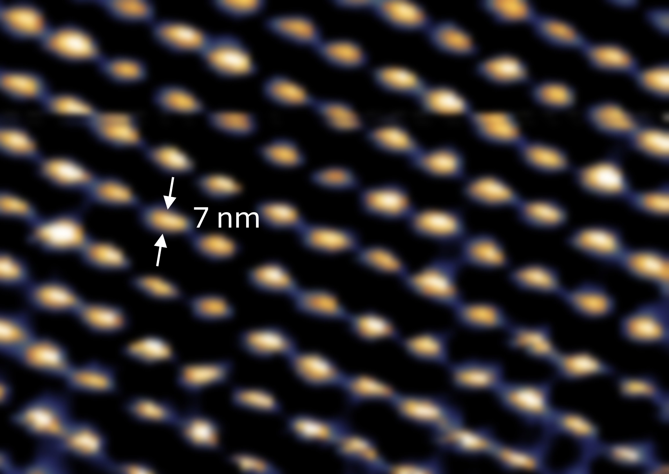
In the QMM Lab, we are pursuing several directions to overcome this crucial scale mismatch: (i) Pushing modern EBL techniques to their limit to achieve few-nanometer feature sizes and tens-of-nanometer superlattice constants, on the scale of electron coherence in many materials (see 'Designer superlattices). (ii) Imparting the symmetry of larger structures down to the atomic scale through ultrafast excitations (see 'Nano-acoustic symmetry engineering'). (iii) Using cavities that are much larger than the lattice but much smaller than the wavelength of resonant light fields to concentrate radiation down and drive novel properties and responses (see 'Vectorial nanocurrents' and 'Cavities').

Image: Atomic force micrograph of silicon dioxide nanopillar array, with feature sizes down to 5 nm (a mere ~10 SiO2 unit cells across) and likely smaller, limited by the probing tip resolution.